BGA Package Introduction
Ball Grid Array packaging technology, high-density I/O connection solution
BGA Package Introduction
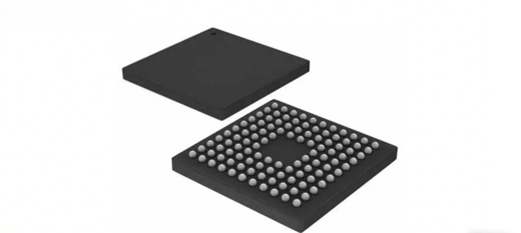
Ball Grid Array packaging, abbreviated as BGA (Ball Grid Array Package), features I/O terminals distributed in array form as circular or cylindrical solder balls under the package. The advantages of BGA technology include: although the number of I/O pins has increased, the pin spacing has not decreased but actually increased, thereby improving assembly yield; although power consumption increases, BGA can use controlled collapse chip connection (C4) soldering to improve its electrothermal performance; thickness and weight are reduced compared to previous packaging technologies; parasitic parameters (output voltage disturbances caused by drastic current changes) are reduced, signal transmission delay is small, and operating frequency is greatly improved; assembly can use coplanar soldering with high reliability.
Product Features
BGA pins consist of an array of solder balls. Using flip chip technology can increase the number of I/Os, with solder balls directly soldered onto the circuit board. Fine solder balls enable more signal, power, and ground interconnections in smaller spaces, making them suitable for high-speed, high-performance integrated circuits. Good thermal performance: Due to its structural characteristics, BGA packaging has good thermal performance. Excellent signal transmission performance: Suitable for applications requiring high-speed signal transmission.
High-Density Interconnection
Allows a large number of pins to be arranged within a small package size, improving integration
Excellent Signal Transmission
Short lead paths reduce inductance and resistance, minimizing signal delay
Good Thermal Performance
Efficient thermal conduction paths optimize electrothermal performance
Process Capability
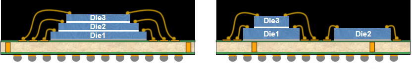
"Sandwich" stacked packaging can achieve ultra-thin chips, multi-layer stacking, and can realize SIP packaging composed of multiple IC chips and different types of components.
| Parameter | Specification |
|---|---|
| Package Size | 5.0*5.0 ~ 15*15mm |
| Package Form | "Sandwich" Stacked Package |
| Process Features | Ultra-thin chips, multi-layer stacking, SIP packaging |
BGA Specifications
| NO. | Lead Count | Body Size | Package Height | Ball | Ball Diameter | Substrate size | Unit/IO |
|---|---|---|---|---|---|---|---|
| 1 | BGA 8*8*0.65 | 8*8 | 0.65 | 121 | 0.3 | 258*78 | 174 |
| 2 | BGA 12*12*0.8 | 5*5.8 | 0.8 | 48 | 0.4 | 240*76.3 | 90 |
| 3 | BGA 14*14*0.65 | 3.5*3.5 | 0.65 | 328 | 0.3 | 126*60 | 64 |
| 4 | BGA 14*14*0.8 | 10.2*10.2 | 0.8 | 289 | 0.4 | 240*76.3 | 64 |
| 5 | BGA 15*17*1.1 | 12.7*10.2 | 1.1 | 165 | 0.45 | 240*76.3 | 90 |
Application Range
Applied in memory, industrial control, medical electronics, environmental detection, information communication and other fields.
Memory
High-performance memory chips and storage solutions
Industrial Control
Automation equipment and industrial control systems
Medical Electronics
Medical monitoring and diagnostic equipment
Environmental Detection
Environmental monitoring and data acquisition equipment
Information Communication
Communication equipment and network infrastructure
Need Customized BGA Packaging Solutions?
DingXin Microelectronics provides comprehensive BGA customization services, from product design, material selection to production testing, meeting your specific needs. Our engineering team will provide professional consultation and technical support.
Contact Us